Continuous monitoring of UV exposure
UV lamps are used to cure coatings and adhesives in many industrial manufacturing processes. And special sensors are used to measure the intensity of the UV light applied to these surfaces. But because these sensors age too quickly, they can only be used to record intermittent measurements. Fraunhofer researchers have developed a new generation of sensors capable of continuously monitoring UV intensity. These devices will be presented for the fi rst time at the Sensor + Test trade show in Nuremberg, from May 14 to 16 (Hall 12, Booth 537).
“UV exposure” is a term that tends to ring alarm bells, as most people associate it with unpleasant consequences such as sunburn and the risk of skin cancer. But ultraviolet (UV) light can also be benefi cial, or indeed essential: the human body needs it to produce vitamin D. Industry, too, makes use of UV light, for example to cure adhesives or the coatings applied to food packaging, and also to disinfect water. On the other hand, surfaces can be damaged if they are exposed to too much UV light, and poorly regulated UV lamps also waste energy and generate excessive amounts of ozone. UV sensors are therefore used to optimize light intensity.
Usually these sensors are made of silicon or silicon carbide. The problem with silicon sensors is that they only deliver useful results if visible light is excluded from the measurement by external fi lters. Unfortunately, the fi lters used are very expensive and not particularly resistant to ultraviolet light. So to reduce ageing, measurements can only be taken intermittently, as snapshots. Silicon carbide sensors have the advantage of being able to withstand longer exposure to UV light, but they only operate in a narrow spectral band. In the majority of industrial curing processes, it is the longer wavelengths that are of interest – precisely the area in which these sensors are least accurate.
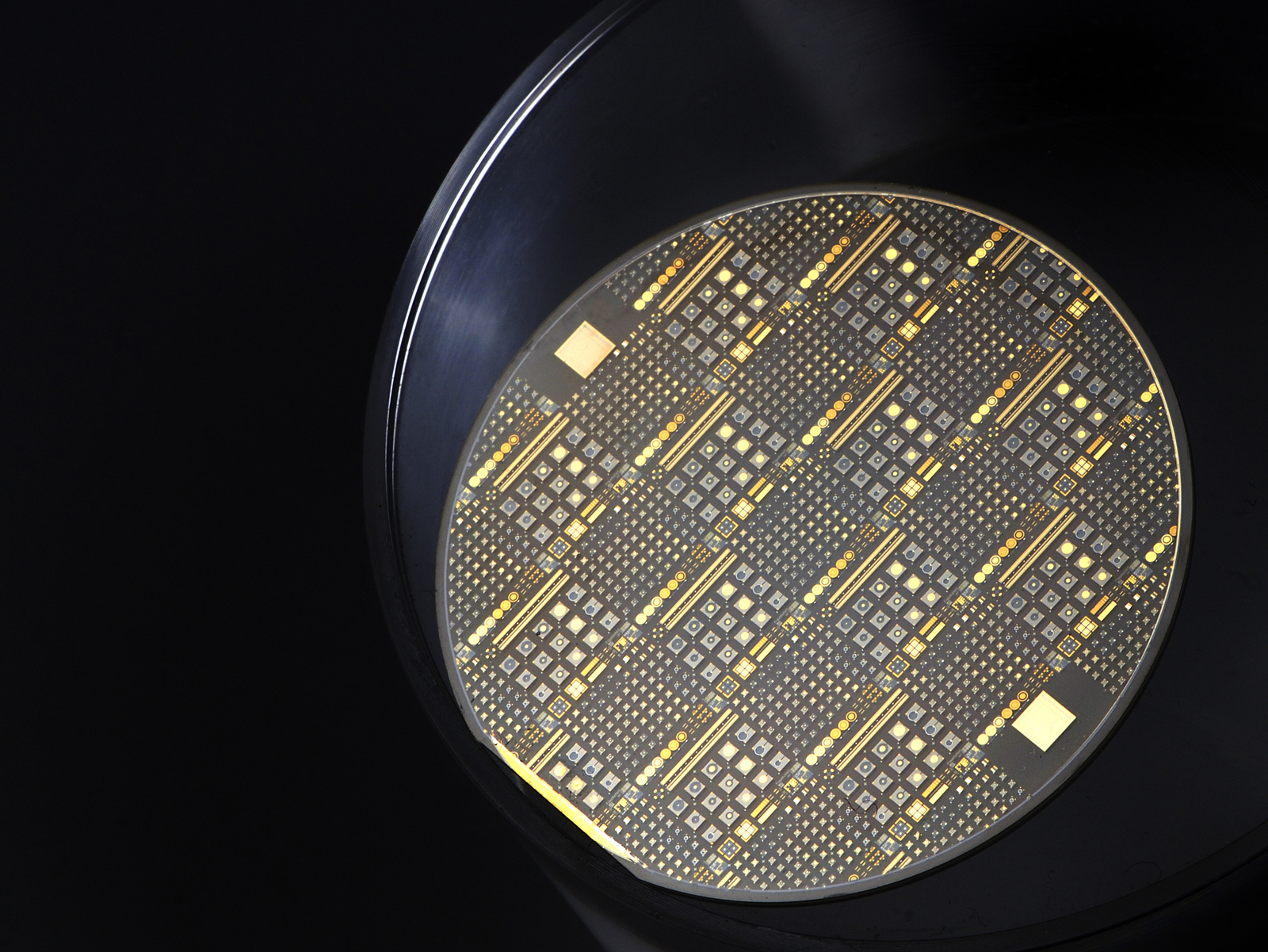
Researchers at the Fraunhofer Institute for Applied Solid State Physics IAF in Freiburg have now developed a new UV sensor in collaboration with colleagues at the Fraunhofer Institutes for Manufacturing Technology and Advanced Materials IFAM, for Optronics, System Technologies and Image Exploitation IOSB, for Silicon Technology ISIT and for Physical Measurement Techniques IPM. “Our sensor is based on aluminum gallium nitride technology and can withstand continuous exposure to UV light without damage,” says IAF project manager Dr. Susanne Kopta. “This enables it to be used not only for intermittent snapshots but also for permanent inline monitoring.” A sapphire wafer serves as the substrate for the sensors. The researchers apply epitaxial growth to deposit layers of the active material onto the substrate, in other words the layers have a crystalline structure.
Sensor for high UV intensities
The particular strength of this novel sensor is its suitability for applications involving very high UV intensities – and for tasks that require the monitoring of specifi c spectral ranges. This is due to the fact that the detectors can be set to operate in two different ways. The fi rst option is to defi ne a maximum wavelength threshold. In this case the sensor detects all UV light emitted at wavelengths below the set limit. The alternative is to defi ne two wavelength thresholds, thus “cutting out” certain parts of the spectrum. “The narrowest range we have been able to achieve is a separation of 20 nanometers,” reports Kopta. This makes it possible to manufacture one sensor for UV-A, another for UV-B, and a third for UV-C. But how do the researchers set the wavelengths to be detected by the sensor? Kopta replies: “We do this by varying the ratio of gallium to aluminum in one of the aluminum gallium nitride layers.”
Defining this ratio is one of the challenges that the researchers are working on at present. Another challenge is growing the aluminum gallium nitride crystal – the heart of the sensor – in such a way that it is free of structural defects and impurities. Failure to do so would result in unreliable measurements because different areas of the sensor would absorb light at different wavelengths. “The hardest part is dealing with the wide range of parameters that affect the manufacture of thin crystal fi lms, which demands a great deal of experience,” explains Kopta.
A few demonstration models have already been produced. In the next stage of the project, the researchers aim to optimize crystal growth and obtain more sharply defi ned wavelength limits. They are also investigating the component durability, with very encouraging results so far. “Initial tests have confi rmed that the sensors are capable of operating for 1000 hours under high UV exposure without suffering any damage,” reports Kopta.
UV sensors as team players
The UV sensors are not only excellent “solo artists”; they are also great team players.By placing more than 100 detectors side by side in a strip, you obtain a UV camera. This device can be used to monitor plasma deposition processes, such as those employed to coat solar cells with an antirefl ective fi lm. The sensor strip can also serve as a spectrometer. In this case, the UV light is fi rst passed through a diffraction grating which splits the light into its various spectral components, like the colors of a rainbow. Each individual sensor detects a specifi c wavelength and provides information on the intensity of light at that wavelength. This would be a good way of conducting ageing tests on the mercury lamps commonly used for water disinfection or UV curing. Does the lamp still emit light of the desired intensity throughout the entire spectrum, or are certain wavelengths weaker than they ought to be?
The researchers will be presenting the novel UV sensors for different wavelengths at the Sensor + Test trade show in Nuremberg from May 14 to 16 (Hall 12, Booth 537).
